Semiconductor wafer bond strength testing is a critical quality control and reliability step for MEMS, 3D integration, SOI substrates, and advanced packaging processes such as hybrid bonding and wafer-level capping. By quantifying tensile strength, shear strength, interfacial fracture energy, and void-free bonding integrity against recognized standards from organizations such as ASTM, ISO, JEDEC, and MIL-STD, accredited third-party laboratories help manufacturers validate bonding processes, screen weak interfaces, and prevent costly delamination failures during dicing, thinning, and thermal cycling.
Technical Overview
Wafer bonding is a foundational process in modern semiconductor manufacturing, in which two substrates are permanently or temporarily joined to form hermetic cavities, stacked die, engineered substrates, or heterogeneously integrated systems. Common bonding technologies include silicon direct (fusion) bonding, plasma-activated bonding, anodic (glass-to-silicon) bonding, eutectic and thermocompression metal bonding, glass frit bonding, polymer adhesive bonding, temporary carrier bonding, and copper/dielectric hybrid bonding used in 3D stacking.
Bond strength directly determines whether a bonded stack survives downstream processes such as grinding, thinning, dicing, wire bonding, reflow, and long-term thermo-mechanical stress. An interface that is under-bonded, contaminated, or affected by voids can delaminate, causing yield loss and latent field failures. Semiconductor wafer bond strength testing therefore measures the mechanical integrity of the interface using both quantitative destructive methods and complementary non-destructive inspection techniques.
Depending on the bonding technology and failure mode of interest, results are expressed as tensile or shear strength in megapascals (MPa), interfacial fracture energy or surface energy in joules per square meter (J/m²), or fracture toughness in MPa·√m. Testing is typically performed in accordance with internationally recognized procedures published by ASTM International, ISO, JEDEC, MIL-STD, EN, JIS, and related standards organizations, and can be carried out by accredited third-party laboratories to support process development, incoming inspection, qualification, and failure analysis.
Testing Samples
Blanket-Bonded Test Wafer Pairs
Full-diameter wafer pairs (100 mm to 300 mm) bonded with unpatterned surfaces, such as silicon-to-silicon, oxide-to-oxide, or silicon-to-glass stacks, are the most common format for process development and statistical bond strength monitoring. Full wafers enable wafer-level strength mapping as well as non-destructive void inspection before destructive coupon testing.
Diced Coupons and Die-Sized Specimens
Blanket or patterned wafers are diced into square or rectangular coupons (typically 5 mm × 5 mm up to 15 mm × 15 mm) for tensile pull, die shear, and fracture mechanics testing. Coupon testing allows many data points to be collected from a single wafer pair and supports statistical evaluation across wafer position, including center, mid-radius, and edge sites.
Patterned Device and Capped MEMS Wafers
Product wafers with real topography, such as MEMS sensor wafers with cap or lid wafers bonded over sealed cavities, vacuum-sealed resonators, and wafer-level packaged image sensors, can be evaluated at die level to verify that seal ring design, metallization, and bond frame geometry deliver the required strength and hermetic quality.
Temporary Bonded and Thinned Stacks
Carrier-to-device stacks bonded with temporary adhesives or laser-release layers are tested to confirm that bond strength is sufficient for thin-wafer handling yet falls within the process window for clean debonding. Both peak strength and failure mode are reported to identify adhesive residue or substrate damage risks.
Dissimilar and Compound Semiconductor Stacks
Heterogeneous integration samples, including glass lids on silicon, quartz, silicon carbide, and III-V compound semiconductor layers transferred onto silicon (such as GaAs or InP on Si for photonic applications), are tested to qualify coefficient-of-thermal-expansion mismatch performance after annealing and temperature cycling.
Testing Items
Typical quantitative and semi-quantitative test items for wafer bond strength evaluation include:
- Tensile pull bond strength (MPa) of diced coupons or full dies
- Die shear and lap shear bond strength (N or MPa)
- Interfacial critical energy release rate, Gc (J/m²), by four-point bend or similar fracture mechanics methods
- Mode I interfacial fracture energy, GIC (J/m²), by double cantilever beam testing
- Fracture toughness, KIC (MPa·√m), by the micro-chevron method
- Bond surface energy (mJ/m² or J/m²) by the blade insertion crack opening method
- Void area percentage and unbonded region mapping by infrared or acoustic imaging
- Failure mode classification (adhesive at the interface, cohesive within the bonding layer, or bulk substrate fracture)
- Strength retention after preconditioning, thermal cycling, high-temperature storage, or moisture exposure
Testing Methods
Tensile Pull-Off Testing
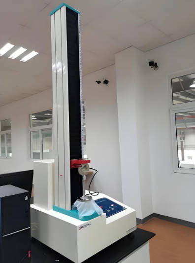
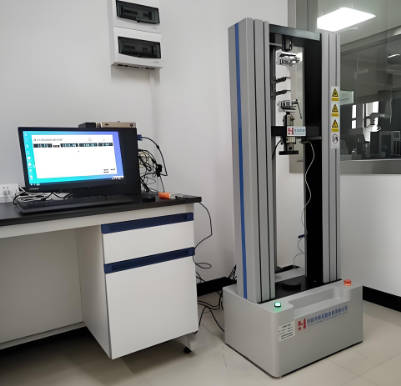
Tensile bond strength is measured by rigidly fixturing a coupon between aligned pull fixtures, often using high-strength epoxy-attached studs following the principles of ASTM D4541 and ASTM C633 adapted for semiconductor specimens. The specimen is loaded in normal tension until fracture, and the maximum stress at failure is calculated from the peak force and bond area. This method is well suited to glass frit, eutectic, adhesive, and anodic bonds, while very strong fusion or hybrid bonds may exceed the adhesive limit and are better evaluated by fracture mechanics methods.
Die Shear Testing
Shear testing per MIL-STD-883 Method 2019 (with equivalent JEDEC and JIS practices) applies a lateral force to a bonded die or coupon using a shear tool at a controlled height and speed. The maximum shear force and calculated shear strength are reported, together with the fracture surface failure mode. Shear testing is highly effective for metal-based and glass frit bond frames and for comparing process splits on patterned product wafers.
Four-Point Bend Interfacial Fracture Testing
The four-point bend method dices a strip specimen, cuts a notch through the top substrate down to the bond interface, and loads the strip in bending to drive a stable interfacial crack. Using beam theory fracture mechanics analysis, the critical energy release rate Gc is extracted. Because of its excellent repeatability and applicability to very strong interfaces, four-point bend testing has become a reference method for hybrid bonding and dielectric/metal interfacial adhesion in 3D integration.
Double Cantilever Beam (DCB) Testing
In the DCB configuration, adapted from Mode I delamination practices such as ASTM D5528, an opening load is applied to the arms of a bonded strip to propagate a crack along the interface. The measured load-displacement data yield the Mode I interfacial fracture energy GIC, making the method valuable for anodic, adhesive, and other high-strength bonds requiring engineering fracture data for reliability modeling.
Micro-Chevron Fracture Toughness Testing
The micro-chevron test uses dedicated test structures in which a chevron-shaped notch is etched into one wafer before bonding. During loading, a crack initiates at the chevron tip and grows stably along the interface, allowing direct determination of fracture toughness KIC with high reproducibility. This method is specifically designed for strong fusion and activated direct bonds whose strength saturates other test methods.
Blade Insertion (Crack Opening) Surface Energy Method
Also known as the crack propagation or blade method, a thin blade of known thickness is inserted into the bond interface to debond a region of the wafer. The equilibrium crack length is measured, typically by infrared imaging, and the bond surface energy is calculated from beam theory as a function of the substrate elastic modulus, wafer thickness, blade thickness, and crack length. This quick, wafer-level technique is ideal for monitoring direct and plasma-activated bonding processes, with well-bonded silicon approaching the bulk silicon cleavage energy of approximately 2 to 2.5 J/m².
Non-Destructive Void and Delamination Inspection
Because local unbonded areas act as strength-limiting defects, non-destructive evaluation is an essential complement to strength measurement. Infrared transmission imaging detects voids and interface particles in bare silicon pairs, scanning acoustic microscopy (C-SAM) maps delaminations and micro-voids in opaque or multi-layer stacks, and X-ray inspection verifies glass frit and metal bond frame coverage. Resulting bond coverage percentages and defect maps are reported alongside quantitative strength data.
Conditioned testing is also available in which coupons are stressed by temperature cycling, high-temperature storage, or damp heat exposure per JEDEC and related guidelines before strength re-testing, quantifying strength degradation over product lifetime.
Applications
Bond strength testing services support a wide range of semiconductor segments and development activities, including:
- MEMS cap wafer and hermetic package qualification for accelerometers, gyroscopes, pressure sensors, microphones, and resonators
- 3D wafer-level stacking and through-silicon via (TSV) integration using metal and hybrid bonding
- High-bandwidth memory and chiplet stacking process qualification
- SOI and engineered substrate manufacturing, including layer transfer and ion-cut process control
- CMOS image sensor wafer-level packaging and wafer-level optics bonding
- Power semiconductor and RF device assembly using glass frit, eutectic, and anodic bonding
- Temporary bonding and debonding process window definition for ultra-thin wafer handling
- Failure analysis, supplier benchmarking, and incoming quality control at foundries, packaging houses, and integrated device manufacturers
FAQ
Which bond strength test method should be selected for my bonding process?
Method selection depends on the bonding class and expected strength. Tensile pull and die shear tests are appropriate for adhesive, glass frit, eutectic, and anodic bonds; four-point bend, double cantilever beam, and micro-chevron tests are recommended for strong direct, plasma-activated, and hybrid bonds; and the blade insertion method provides fast wafer-level surface energy monitoring. Testing engineers can recommend a protocol based on the stack materials and failure criteria.
What are typical target values for wafer bond strength?
Targets are process specific, but well-executed silicon fusion and plasma-activated bonds typically reach 1 to 2.5 J/m², approaching bulk silicon fracture energy; glass frit and eutectic bonds commonly fall in the range of 15 to 50 MPa in tensile or shear testing; and hybrid bonding processes are usually qualified against a defined Gc threshold measured by four-point bend testing. When specimens fail in the bulk substrate rather than at the interface, results are reported as exceeding the substrate strength.
How many samples are required for a statistically meaningful evaluation?
For coupon-level testing, a minimum of ten to twenty specimens distributed across the wafer is recommended so that center-to-edge strength variation and scatter can be assessed. Fracture mechanics methods such as four-point bend and micro-chevron typically require fewer dedicated specimens per condition because of their higher repeatability.
Can full product wafers be tested non-destructively?
Yes. Infrared transmission imaging and scanning acoustic microscopy provide full-wafer bond coverage maps, void percentages, and delamination detection without destroying the wafer. Many programs combine non-destructive wafer mapping with destructive coupon testing to correlate global integrity with local strength.
How is failure mode analyzed after testing?
After each destructive test, fracture surfaces are examined microscopically to classify the failure as adhesive (separation at the bond interface), cohesive (fracture within the bonding layer), or substrate fracture. This classification is as important as the numeric strength value because it identifies the weak link and guides process optimization.
Can bond strength be measured after reliability stress?
Yes. Coupons or wafers can be subjected to temperature cycling, high-temperature storage, or damp heat conditioning per JEDEC and related standards before re-testing, allowing degradation trends and long-term reliability margins to be quantified.
What wafer sizes and specimen formats are accepted?
Testing typically supports wafer diameters from 100 mm to 300 mm as well as pre-diced coupons, individual capped dies, and strip specimens prepared for fracture mechanics testing. Sample preparation, including dicing and notch creation for four-point bend specimens, can often be arranged through the testing laboratory.