Wafer bond strength micro-tensile testing is a quantitative mechanical characterization technique used to measure the adhesion strength of bonded wafer pairs in semiconductor, MEMS, and advanced packaging manufacturing. By applying a controlled uniaxial tensile load to small diced specimens until fracture, the method delivers precise tensile strength data, failure mode classification, and bond uniformity mapping essential for process development and reliability qualification. This article explains the test principle, specimen preparation, applicable standards, and typical applications of micro-tensile testing for wafer bonds.
Technical Overview
Wafer bonding has become a foundational process step in modern microelectronics, enabling device stacking, hermetic encapsulation, and heterogeneous integration in MEMS, 3D ICs, CMOS image sensors, SOI substrates, and power devices. Because the mechanical integrity of a bonded interface directly determines yield, long-term reliability, and hermetic performance, accurate quantification of bond strength is essential at every stage, from early process development to final production qualification.
Micro-tensile testing is a destructive evaluation method in which small specimens, typically individual dice or narrow strips diced from a bonded wafer pair, are gripped on both opposing sides and pulled apart along a uniaxial loading axis until the bond interface fails. The maximum recorded force at fracture, divided by the effective bonded area, yields the tensile bond strength in megapascals (MPa). Compared with qualitative or semi-quantitative approaches such as blade insertion, wedge opening, or tensile pull of large coupons, micro-tensile testing provides statistically analyzable numerical results, well-defined failure modes, and the ability to map strength uniformity across an entire wafer.
The technique is applicable to virtually all bonding technologies, including silicon direct (fusion) bonding, plasma-activated bonding, anodic bonding, adhesive bonding, glass frit bonding, eutectic and solder bonding, and metal–metal hybrid bonding. Testing is typically performed in accredited third-party laboratories or corporate reliability laboratories following internationally recognized frameworks published by standards organizations such as SEMI, ASTM, JEDEC, and MIL-STD.
Testing Samples
Full Bonded Wafer Pairs
Complete bonded wafer pairs with diameters of 150 mm, 200 mm, or 300 mm can be submitted for evaluation. Engineers define a sampling plan that targets center, mid-radius, and edge locations so that radial bond uniformity can be assessed. The wafers are subsequently diced into individual test specimens according to the agreed sampling layout.
Diced Die and Strip Specimens
The most common specimen format is the diced coupon, typically square or rectangular sections ranging from approximately 2 mm × 2 mm up to 10 mm × 10 mm, or strips a few millimeters in width. Each specimen retains the full multilayer bonded stack, and the diced edges provide defined regions for fixture engagement and load transfer. Specimen geometry is selected to balance statistical sampling density against the practical limits of handling and alignment.
Bond Types and Material Combinations
- Silicon–silicon fusion or plasma-activated direct bonds
- Silicon–glass or glass–silicon anodic bonds
- Adhesive bonds using benzocyclobutene (BCB), polyimide (PI), or other polymer interlayers
- Glass frit bonds used for MEMS capping and hermetic sealing
- Eutectic bonds such as Au–Si and Au–Sn, and solder-based interconnects
- Copper–copper, aluminum–aluminum, or hybrid metal/dielectric direct bonds for 3D integration
Patterned and Structured Specimens
Specimens containing real product features, including cavities, sealing rings, through-silicon via (TSV) arrays, and patterned metallization, can be tested to characterize bond strength under conditions that closely represent actual device geometry, rather than relying solely on blanket-bonded layers.
Testing Items
The core measured and reported parameters of a micro-tensile bond strength study include the following:
- Tensile bond strength (MPa), defined as the maximum tensile stress sustained by the interface before fracture
- Peak fracture force (N or kgf), the raw maximum load recorded during the pull event
- Shear bond strength (MPa), when shear loading is evaluated in addition to or instead of tensile loading
- Effective bonded area and bond coverage ratio, determined from post-test fracture surface inspection
- Failure mode classification, distinguishing adhesive failure at the interface, cohesive failure within the bonding layer, and bulk fracture of the substrate material
- Bond uniformity mapping as a function of wafer position
- Statistical characterization, including mean strength, standard deviation, and Weibull distribution parameters for brittle failure populations
Optional deliverables include fractographic examination of the separated surfaces by optical microscopy or scanning electron microscopy (SEM) to quantify void density, unbonded regions, and crack initiation sites. This is particularly important for direct-bonded and hybrid-bonded interfaces, where the effective bonded area can differ significantly from the nominal die area.
Testing Methods
Specimen Preparation
Bonded wafers are first singulated using a precision dicing saw with parameters selected to minimize chipping and delamination at the bond line. Diced specimens are cleaned to remove dicing debris and moisture, and their bonded dimensions are measured for accurate stress calculation. Specimens are then attached to load-transferring fixtures or carriers using high-strength structural adhesives whose strength reliably exceeds the expected wafer bond strength, ensuring that fracture occurs at the bond interface under investigation rather than at the grip or mounting interface. Complete curing of the mounting adhesive under controlled conditions is verified before testing.
Instrumentation and Fixtures
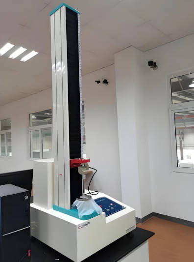
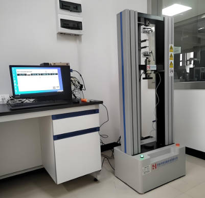
Testing is performed on a micro-force universal testing machine or a dedicated die pull/shear tester equipped with a low-capacity, high-resolution load cell, typically in the range of a few hundred newtons with millinewton-level resolution. Self-aligning grippers and articulated fixtures are used to keep the loading axis perpendicular to the bond plane and to minimize parasitic peel moments and bending stresses, which can otherwise underestimate true strength. Tests are conducted under displacement control at a constant crosshead speed, commonly in the range of 0.1 to 1 mm/min or as specified by the governing standard, at room ambient laboratory conditions unless environmental testing is specifically required.
Test Procedure
- Mount the prepared specimen and verify that the pull axis is aligned perpendicular to the bonded interface
- Apply a small preload and zero the load cell and displacement readings
- Extend the actuator at constant rate while continuously recording the load–displacement curve
- Capture the peak force at the moment of fracture
- Inspect both fracture surfaces under microscopy, classify the failure mode, and determine the effective bonded area
- Calculate tensile bond strength as peak force divided by effective bonded area
- Repeat for all specimens in the sampling plan and compile results statistically
Data Evaluation and Acceptance Criteria
Individual strength values are aggregated to produce mean strength, distribution width, and, where appropriate, Weibull characteristic strength and modulus. Results are compared against internal specifications or industry-recognized reference values, such as the minimum die attach strength levels referenced in military and JEDEC test method documents. A clear pass or fail statement, together with the failure mode distribution, is provided in the final test report, enabling engineering teams to trace root causes such as surface contamination, insufficient annealing, or non-optimized plasma activation.
Applications
Micro-tensile bond strength testing supports a wide range of engineering and quality activities across the semiconductor value chain:
- MEMS capping and hermetic encapsulation process qualification
- Wafer-level 3D stacking and through-silicon via (TSV) integration for 3D ICs
- CMOS image sensor wafer-to-wafer stacking and layer transfer verification
- SOI and engineered substrate manufacturing quality control
- Power device and wide-bandgap semiconductor wafer bonding evaluation
- Advanced packaging formats, including fan-out wafer-level packaging and chiplet heterogeneous integration
- Process window development, such as plasma activation parameters, surface preparation chemistry, and annealing temperature optimization
- Reliability qualification, supplier incoming inspection, and failure analysis root-cause studies
Because the method uses small diced specimens, it is equally suitable for characterization of engineering lots during development and for routine statistical process control in production, where wafer-level bond uniformity trends provide early warning of process drift.
FAQ
What strength levels can be expected for different bond types?
Fully annealed silicon fusion bonds can approach the fracture strength of bulk silicon, often causing failure within the substrate rather than at the interface. Anodic bonds typically exhibit strengths in the range of 10 to 30 MPa, while adhesive bonds commonly measure between approximately 5 and 50 MPa depending on the polymer system and cure conditions. Actual values depend strongly on bond coverage, void density, and surface preparation quality.
How many specimens are needed for a valid evaluation?
A statistically meaningful study generally includes at least 10 to 30 diced specimens per wafer, distributed across multiple wafer locations. Larger sample counts are recommended when Weibull characterization is required, when comparing process splits, or when strength distributions are expected to be wide due to partial bonding or voids.
How does micro-tensile testing compare with die shear and blade insertion methods?
Die shear testing, standardized in documents such as JEDEC and MIL-STD-883 test methods, applies a lateral shear load and is best suited to die-attach and capped device geometries. Blade or wedge insertion methods estimate surface energy from crack length and are quick but sensitive to operator technique and specimen stiffness. Micro-tensile testing provides a direct, quantitative tensile strength value with clear failure mode information, making it the preferred method for detailed bond interface characterization and process comparison.
Which standards and reference documents are relevant?
While no single international standard exclusively governs wafer bond micro-tensile testing, established frameworks from SEMI, ASTM, JEDEC, and MIL-STD-883 for die shear, bond strength, and adhesion testing are widely adapted as the basis for test plans. Accredited third-party laboratories typically construct test procedures that align with these frameworks while tailoring specimen geometry, fixturing, and acceptance criteria to the specific bonding technology under evaluation.
Can weakly bonded or partially bonded wafers be tested?
Yes. Fixturing and handling protocols are designed for fragile specimens, and low-load-range force sensors allow accurate measurement of very weak bonds. In such cases, fractographic determination of the effective bonded area is especially important, because the nominal die area can significantly overstate the true bonded region and thereby underestimate the intrinsic interface strength.